PCB
To draw the schematics and the layout of the 4-layer PCB, the open-source KiCad suite 1 was used. The first prototype PCB has been built (see Fig. 1) and tested; as the thin purple wires attest, a number of bugs have been spotted and fixed as a result.
Note
It is worth noting here that the components used in this first prototype are not the ones that will be used in the next one; only a few have been picked out of the CERN radiation test database 2, whereas all components will be radiation-tested in the next version.
Note
The dimensions of this prototype are 63mm \(\times\) 38mm. Although this is already quite compact, half of that space is dedicated to the fan driving circuitry. Consequently, a separate revision without fan driving capabilities is planned to ease the integration with the passively-cooled PSU 3.
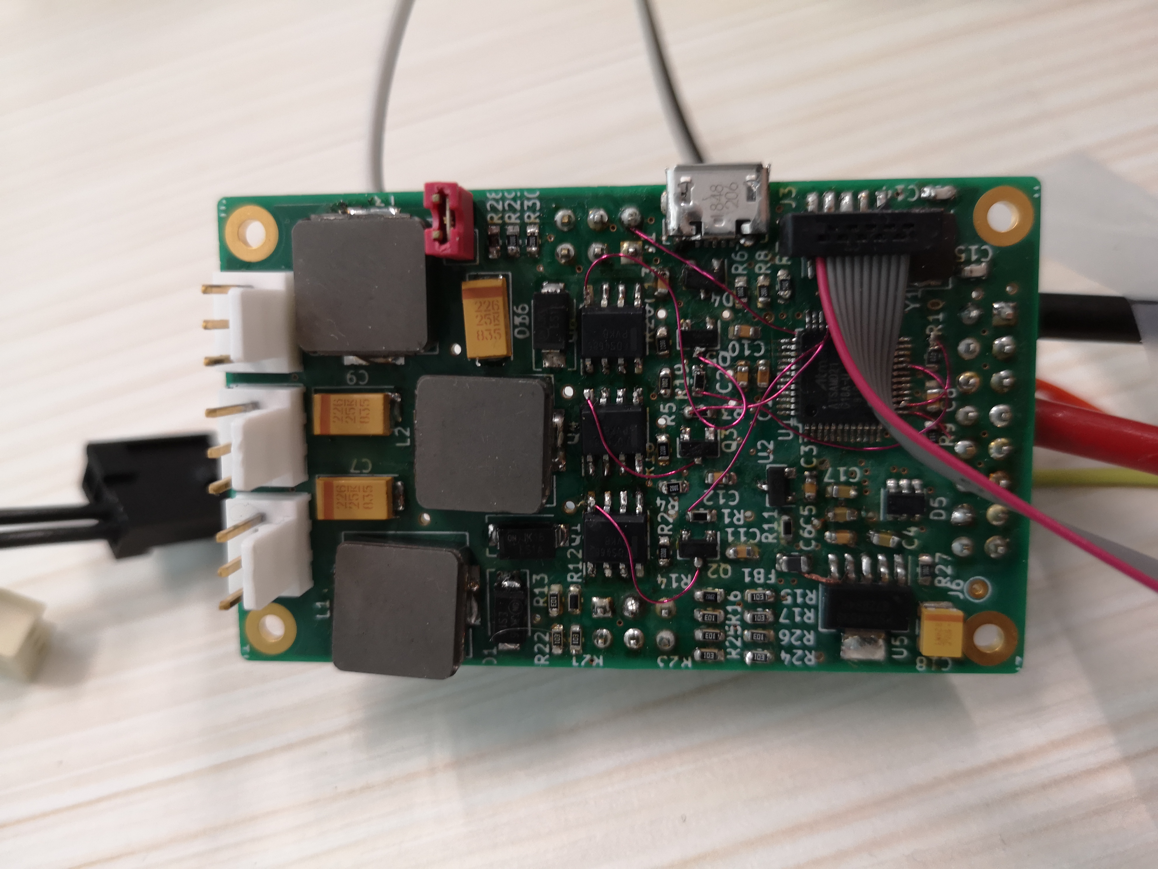
Fig. 1 The first MoniMod prototype
Main blocks
Linear Regulator
The MoniMod is powered by a 5V rail, but the uC needs a power supply between 1.62V and 3.63V to operate; on the other side, SMBus (which defines the electrical characteristics of PMBus) has a power supply range of 3V to 5V (\(\pm\) 10%). To satisfy these constraints, the uC can be operated at 3.3V.
Since its current consumption can be quite low (found to be ~40–45mA) it is enough to use a simple linear regulator to generate this power rail: the TPS7A4533 has been selected from 2.
SAMD21 uC
To power the uC, 1uF and 0.1uF bypass capacitors are placed close to the digital power supply pins; a ferrite bead is used to decouple the 3.3V analog domain from the noise in the digital one.
The uC clock is provided by a 8MHz crystal.
A Micro USB Type B connector allows one to use the USB peripheral of the uC for firmware debugging reasons; a TVS array protects the device from any ESD events. Also, a SWD (Serial Wire Debug) interface is exposed in an on-board header and an external connector.
Fan drivers
Fan driving circuitry has been designed to modulate the DC voltage of the fans such that speed control can be exercised on non-PWM capable models. To convert the 25kHz PWM signals from the uC to DC levels, a buck topology has been used (see Fig. 2).
Components selection allows using 12V fans at 1A maximum current; this is the reason for the quite bulky inductors that can be seen in Fig. 1. Also, this topology might allow a large inrush current if the PWM duty cycle were to change too rapidly; this is handled in the software, which forces it to only change slowly.
Note
Here, a PMOS device has been used; this will be replaced with a radiation-tested high gate driver and NMOS combination.
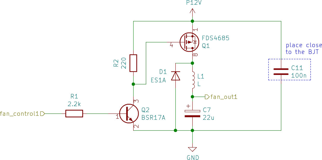
Fig. 2 Schematic of the fan driver buck circuit
Analog inputs
Due to an ADC and an analog MUX being integrated in the uC and the benefit of having as few components as possible (less points of failure in radiation), the analog frontend is very simple: it is just resistor dividers. An impedance of 100k is high enough to keep the quiescent current negligible, and since this is designed to measure levels in the system PSU and not some ultralow noise power supply, it is also sufficient to decouple the potentially noisy switching capacitor analog MUX inside the uC from the signal source.
Note
The temperature sensors are currently of the LM61 type, not requiring any biasing, but in the next revision an optionally mounted current source will be added to enable using PT100 / PT1000 sources.
Connections
The interface between the MoniMod and the system board is contained in connector J2. A limit of 1A per pin requires the use of multiple pins for the 12V supply, since at full speed the fans could draw up to 3A of current.
pin |
name |
pin |
name |
|---|---|---|---|
1 |
GND |
2 |
GND |
3 |
RST_N |
4 |
P12V |
5 |
M_SCL |
6 |
GND |
7 |
P5V |
8 |
P12V |
9 |
M_SDA |
10 |
GND |
11 |
M_IO1 |
12 |
P12V |
13 |
M_IO2 |
14 |
GND |
15 |
GND |
16 |
P12V |
Connector J3 can be used to program and debug the uC using an SWD debugger (like the J-Link EDU Mini).
pin |
name |
pin |
name |
|---|---|---|---|
1 |
P3V3 |
2 |
PGM_SWDIO |
3 |
GND |
4 |
PGM_SWCLK |
5 |
GND |
6 |
N/C |
7 |
N/C |
8 |
N/C |
9 |
N/C |
10 |
PGM_RST_N |
Connectors J4 and J5 are used to configure the PMBus address the MoniMod will assume, and to connect it to what it is monitoring: the temperature sensors; the voltage rails; and the current sense outputs.
Note
In the current version, the current sense just reads an absolute voltage; the next revision shall include a simple opamp-based circuit to read a standard high-side sense resistor.
pin |
name |
pin |
name |
|---|---|---|---|
1 |
TMP1 |
2 |
ADDR0 |
3 |
TMP2 |
4 |
ADDR1 |
5 |
TMP3 |
6 |
ADDR2 |
pin |
name |
pin |
name |
|---|---|---|---|
1 |
V1 |
2 |
I1 |
3 |
V2 |
4 |
I2 |
5 |
V3 |
6 |
I3 |
- 1
KiCad EDA home page: http://www.kicad-pcb.org/
- 2(1,2)
CERN radiation test database: https://radwg-table.web.cern.ch/public/
- 3
RaToPUS home: https://ohwr.org/project/psu-rad-acdc-230v-12v5v-110w/wikis/home