PCB
To draw the schematics and the layout of the 4-layer PCB, the open-source KiCad suite 1 was used. The first prototype PCB has been built (see Fig. 1) and tested; as the thin purple wires attest, a number of bugs have been spotted and fixed as a result.
Note
The dimensions of this prototype are 1.53in \(\times\) 3.14in. Although this is already quite compact, half of that space is dedicated to the fan driving circuitry. Consequently, a separate revision without fan driving capabilities is planned to ease the integration with the passively-cooled PSU 3. Also, in case PT100-type temperature sensors are not eventually used, further size reductions are expected.
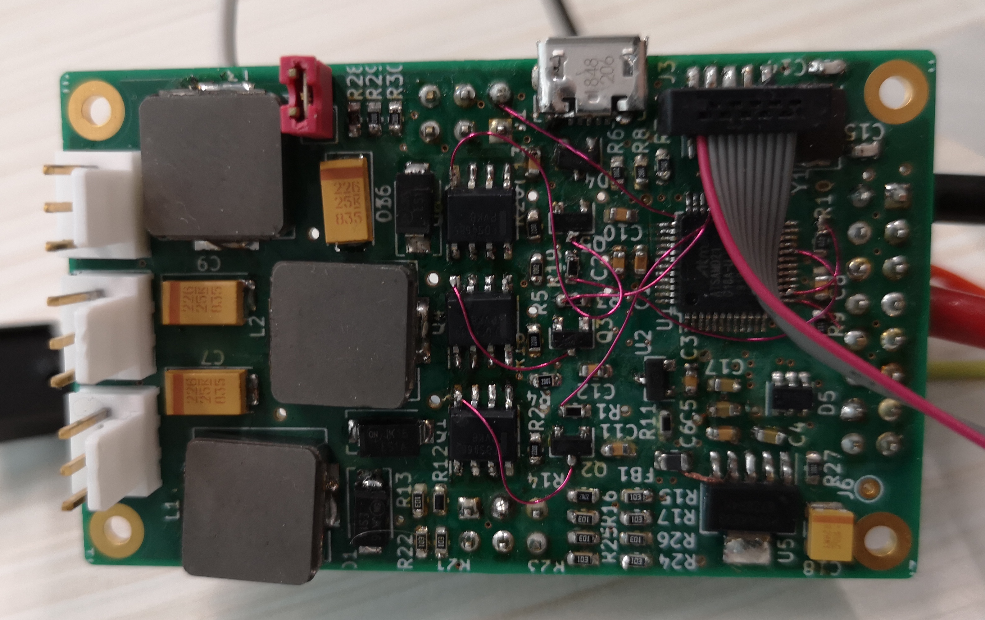
Fig. 1 The first MoniMod prototype
Main blocks
Linear Regulator
The MoniMod is powered by a 5V rail, but the uC needs a power supply between 1.62V and 3.63V to operate; on the other side, SMBus (which defines the electrical characteristics of PMBus) has a power supply range of 3V to 5V (\(\pm\) 10%). To satisfy these constraints, the uC can be operated at 3.3V.
Since its current consumption can be quite low (found to be ~40–45mA) it is enough to use a simple linear regulator to generate this power rail: the TPS7A4533 has been selected from 2.
SAMD21 uC
To power the uC, 1uF and 0.1uF bypass capacitors are placed close to the digital power supply pins; a ferrite bead is used to decouple the 3.3V analog domain from the noise in the digital one.
The uC clock is provided by a 8MHz crystal.
A Micro USB Type B connector allows one to use the USB peripheral of the uC for firmware debugging reasons; a TVS array protects the device from any ESD events. Also, a SWD (Serial Wire Debug) interface is exposed in an on-board header and an external connector.
Fan drivers
Fan driving circuitry has been designed to modulate the DC voltage of the fans such that speed control can be exercised on non-PWM capable models. To convert the 25kHz PWM signals from the uC to DC levels, a buck topology has been used (see Fig. 2).
Components selection allows using 12V fans at 1A maximum current; this is the reason for the quite bulky inductors that can be seen in Fig. 1. Also, this topology might allow a large inrush current if the PWM duty cycle were to change too rapidly; this is handled in the software, which limits the rate of change of the duty cycle.
Note
In the v1 prototype a PMOS device was used, with a BJT driving it. This has been replaced due to the lack of suitable (low Ron) devices that are also radiation-tested.
Note
The low-side driver is not needed here but it is used in the RaToPUS power supply: we use common components where possible because of the high cost associated with qualifying them.
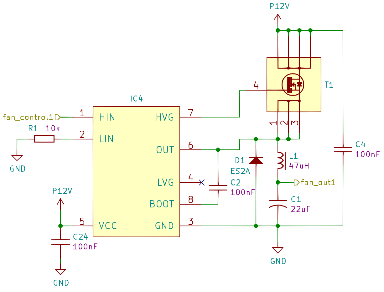
Fig. 2 Schematic of the fan driver buck circuit
Analog inputs
Due to an ADC and an analog MUX being integrated in the uC and the benefit of having as few components as possible (less points of failure in radiation), the analog frontend is kept simple; its basic building blocks are documented below.
Voltage sensing
For the voltage inputs, an impedance of the order of some 10ks is high enough to keep the quiescent current negligible, and since this is designed to measure levels in the system PSU and not some ultralow noise power supply, it is also sufficient to decouple the potentially noisy switching capacitor analog MUX inside the uC from the signal source.
Current sensing
The current sensing uses the differential amplifier in Fig. 3 to lower the voltage difference in the sense resistor (on the host board) and amplify it to a level suitable for sampling with the ADC.
The primary degradation in BJTs exposed in radiation is a reduction in their forward current gain; in this circuit the opamp can easily provide the extra current so the performance should not degrade too much over time.
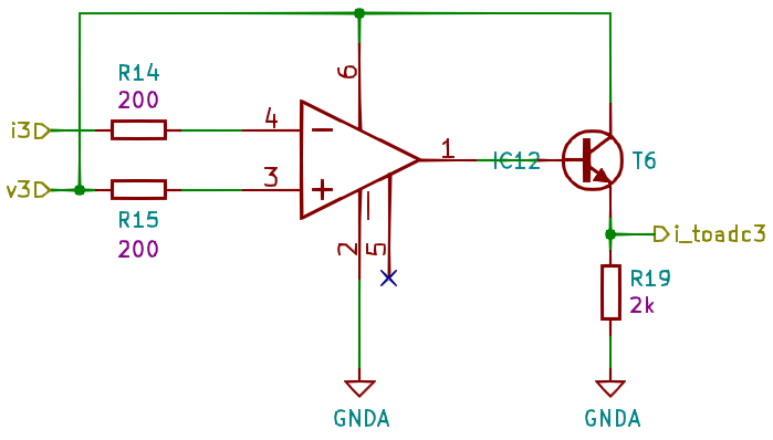
Fig. 3 Schematic of the current sensing circuit
Temperature sensing
In the v2 prototype version, the user can switch between LM61-type and PT100 / PT1000 temperature sensors using the three switches in the back side of the board. This allows comparing the two different solutions under the same conditions (under radiation) and making an informed decision on which type to use in the next version.
As seen on Fig. 4, when the user selects the PT100 option the switch connects a current reference implemented with the Vref and one half of an AD8030 rail-to-rail opamp. The same node is connected to a x15 amplifier, implemented using the other half of the opamp. When the user selects LM61 operation, the switch disconnects the current source and the amplifier such that the sensor input is connected directly to the ADC input.
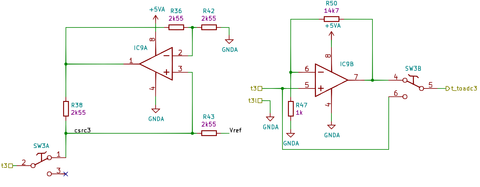
Fig. 4 Schematic of the temperature sensing circuit
Connections
The interface between the MoniMod and the system board is contained in connector J2. A limit of 1A per pin requires the use of multiple pins for the 12V supply, since at full speed the fans could draw up to 3A of current.
pin |
name |
pin |
name |
|---|---|---|---|
1 |
GND |
2 |
GND |
3 |
RST_N |
4 |
P12V |
5 |
M_SCL |
6 |
GND |
7 |
P5V |
8 |
P12V |
9 |
M_SDA |
10 |
GND |
11 |
M_IO1 |
12 |
P12V |
13 |
M_IO2 |
14 |
GND |
15 |
GND |
16 |
P12V |
Connector J3 can be used to program and debug the uC using an SWD debugger (like the J-Link EDU Mini).
pin |
name |
pin |
name |
|---|---|---|---|
1 |
P3V3 |
2 |
PGM_SWDIO |
3 |
GND |
4 |
PGM_SWCLK |
5 |
GND |
6 |
N/C |
7 |
N/C |
8 |
N/C |
9 |
N/C |
10 |
PGM_RST_N |
Connectors J4 and J5 are used to configure the PMBus address the MoniMod will assume, and to connect it to what it is monitoring: the temperature sensors; the voltage rails; and the current sense outputs.
Note
In the current version, the current sense just reads an absolute voltage; the next revision shall include a simple opamp-based circuit to read a standard high-side sense resistor.
pin |
name |
pin |
name |
|---|---|---|---|
1 |
TMP1 |
2 |
TMP1_N |
3 |
TMP2 |
4 |
TMP2_N |
5 |
TMP3 |
6 |
TMP3_N |
pin |
name |
pin |
name |
|---|---|---|---|
1 |
V1 |
2 |
I1 |
3 |
V2 |
4 |
I2 |
5 |
V3 |
6 |
I3 |
pin |
name |
|---|---|
1 |
ADDR0 |
3 |
ADDR1 |
5 |
ADDR2 |
Radiation qualification
Since the board will need to be qualified against radiation effects, it helps if it is comprised of components that are already qualified; for that reason, parts from the CERN radiation test database were preferred. Table 6 shows the list of active components, along with the tests that have been performed for each one. Some possible deployment locations, along with their radiation levels, are listed on Table 8.
Name |
Function |
EDMS Rad Test # |
Rad Test Type |
|---|---|---|---|
TL431BQDBZ |
Reference Voltage |
1171338 |
TID, SEE |
TPS7A4533DCQ |
Linear Regulator |
1911630 |
TID, SEE |
AD8030ARZ |
Dual rail-to-rail opamp |
1729078 |
TID, SEE |
AD8029AKSZ |
rail-to-rail opamp |
1729078 |
TID, SEE |
IRFH5025TRPBF |
N-channel Power MOSFET |
2207602 |
TID, SEE |
BC817-25 |
npn BJT |
1583307 |
TID |
ATSAMD21G18A |
uC |
N/A |
N/A |
L6498D |
Gate driver |
N/A |
N/A |
Note
The uC report hasn’t been uploaded to the radiation database yet but it has been tested, with encouraging results.
Note
The gate driver has not been tested yet, but a number of similar components is scheduled to be tested. In case the selected component proves to be unsuitable, we can be confident that there will be another, similar one, that will replace it at the next version of the PCB.
On the other hand, some components, such as TVS diodes, do not degrade in a way that would impact the design. As such, they have been selected freely. These are listed on Table 7.
Name |
Function |
|---|---|
ES2A |
Fast Recovery Diode |
PESD24VS5UD |
TVS Diodes |
PESD5V0S2UAT |
TVS Diodes |
Location |
Dose [Gy/y] |
HEH [pp / cm 2 / y] |
1MeV [n / cm 2 / y] |
|---|---|---|---|
UJ |
10 |
5e9 |
5e10 |
UL |
0.2 |
1e8 |
1e9 |
RR alcoves |
6 |
3e9 |
3e10 |
ARC |
2 |
1e9 |
1e9 |
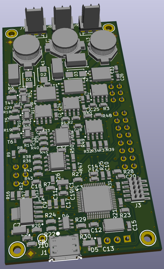
Fig. 5 A rendering of the second MoniMod prototype
- 1
KiCad EDA home page: http://www.kicad-pcb.org/
- 2
CERN radiation test database: https://radwg-table.web.cern.ch/public/
- 3
RaToPUS home: https://ohwr.org/project/psu-rad-acdc-230v-12v5v-110w/wikis/home
- 4
LHC and HL-LHC: Present and Future Radiation Environment in the High-Luminosity Collision Points and RHA Implications: https://ieeexplore.ieee.org/document/8116686